
The semiconductor industry is constantly evolving to meet the increasing demands for higher performance and efficiency. Two of the most important innovations in this area are high bandwidth memory (HBM) and 3D stacking1. Although both technologies are no longer "new" (HBM was launched on the market in 2013, 3D stacking was even developed in the early 2000s), the insanely increasing demand for more compact and powerful chips has made them considerably more important2.
The increasing demand for HBM and 3D stacking can be attributed to the boom in artificial intelligence (AI) and high-performance computing (HPC) applications, among other things. According to a study by IDC, the market for HBM and related technologies is expected to reach an annual growth rate of over 20% by 20243.
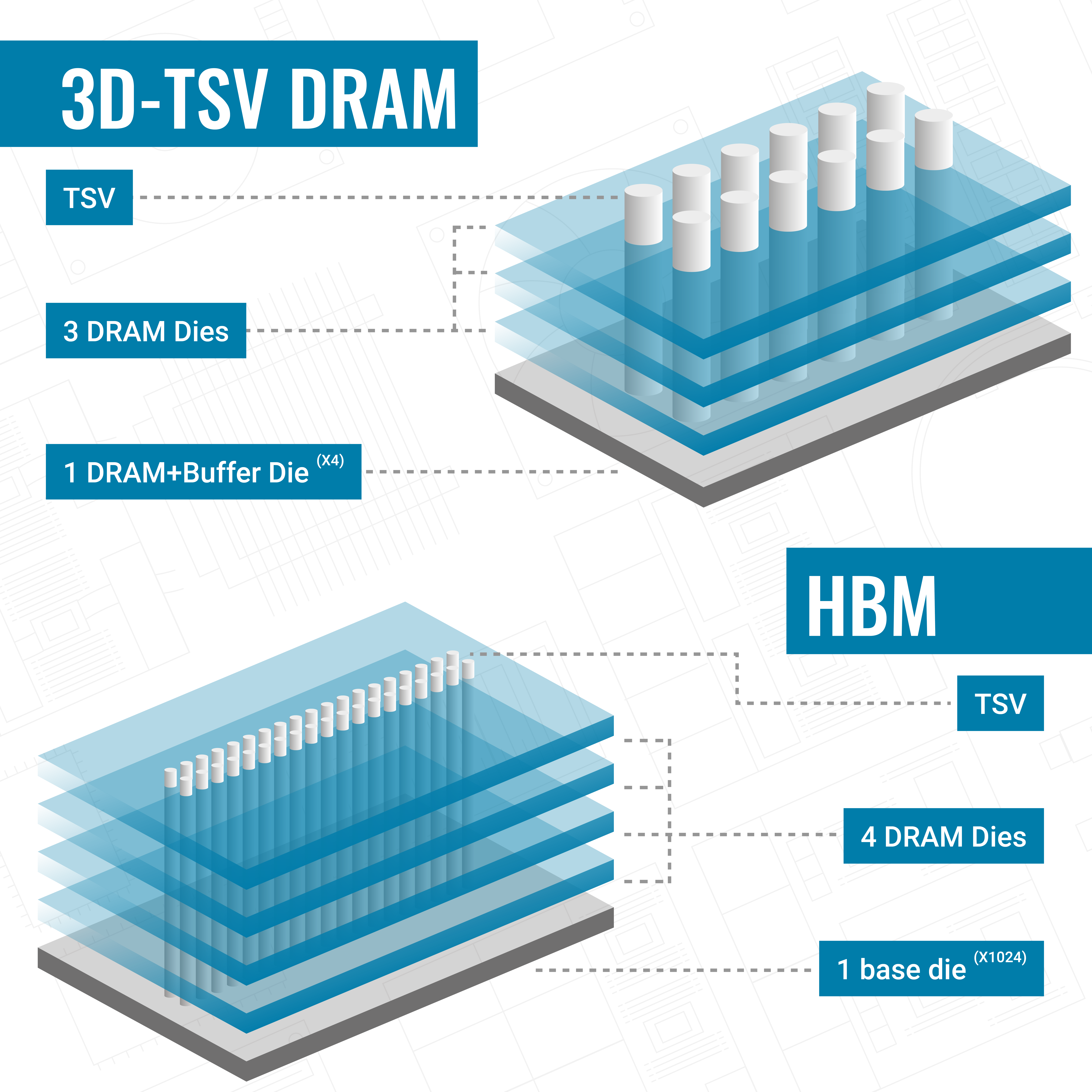
What is 3D stacking?
3D stacking is a technology in which several semiconductor chips are stacked on top of each other and connected by vertical connections, so-called "through-silicon vias" (TSVs). This technology enables a significant reduction in latency and an increase in bandwidth, as the signals only have to travel short distances.
"Traditional" arrangement of semiconductor chips
Semiconductor chips are usually arranged next to each other on a printed circuit board (PCB). This arrangement requires longer connection paths between the chips and the memory controller or processor, which leads to higher latency times and increased energy consumption. In addition, this horizontal arrangement takes up more space, which limits the miniaturization and power density of electronic devices.
Advantages of 3D stacking:
- Increased performance:
Vertical integration of the chips can minimize signal propagation times and improve performance. - Space saving:
Stacking several chips on top of each other saves space and enables more compact designs. - Energy efficiency:
As with HBM, the proximity of the chips to each other reduces energy consumption.
3D stacking is used in various areas, including memory technology, processors and special AI chips. This technology is particularly relevant for applications that have high performance requirements and also need compact and energy-efficient solutions.
1https://kpmg.com/us/en/articles/2024/global-semiconductor-industry-outlook.html2https://www2.deloitte.com/us/en/pages/technology-media-and-telecommunications/articles/semiconductor-industry-outlook.html
3https://www.idc.com/getdoc.jsp?containerId=prAP51603223
What is High Bandwidth Memory (HBM)?
High Bandwidth Memory (HBM) is an advanced form of DRAM memory designed to offer higher bandwidth and energy efficiency than traditional DRAM modules.
A conventional DRAM module consists of several memory chips, which - as explained above - are arranged horizontally on a printed circuit board (PCB). This arrangement leads to longer connection paths between the chips and the memory controller, which can limit the data transfer speed and increase energy consumption.
HBM, on the other hand, uses vertical stacks of memory chips that are interconnected by so-called through-silicon vias (TSVs). This allows the chips to be closer together and therefore shorter connection paths, which increases the data transfer speed and reduces energy consumption.
Short and sweet: HBM and 3D stacking
- 3D Stacking:
Semiconductor chips stacked on top of each other, connected by TSVs. - HBM:
Vertical stacking of DRAM chips, connected by TSVs. - Advantages:
Higher performance, space saving, energy efficiency. - Areas of application:
memory technology, processors, AI chips, HPC.
HBM technologies, relevance and availability
High Bandwidth Memory (HBM) has established itself as a key technology in the memory market, particularly in the field of high-performance computing (HPC) and artificial intelligence (AI). Thanks to its high bandwidth and energy efficiency, HBM enables a significant increase in performance while reducing energy consumption at the same time. These properties make HBM ideal for applications that need to process large amounts of data quickly, such as in supercomputers, AI accelerators and advanced graphics processing units (GPUs)4 .
4https://www.hpcwire.com/2024/03/06/memcon-2024-insights-into-cxl-hbm-genai-and-more/Relevance and availability of HBM
High Bandwidth Memory (HBM) has established itself as an extremely relevant technology, especially in areas such as artificial intelligence (AI) and high performance computing (HPC). Leading cloud providers such as Amazon Web Services (AWS) and Google are already using HBM in their cloud services and specialized computing resources to provide the high computing power and efficiency that modern applications require5,6.
HBM has so far mainly been used in absolute high-end products such as NVIDIA's H200 GPUs and AMD's Radeon Instinct MI100 and MI200. However, HBM is not currently available in the form of standalone modules for direct purchase. There are currently no announcements from manufacturers that such modules will be coming to market in the near future. HBM development and production is currently focused on integration into specialized high-performance products.
Although the availability of HBM for the broad market is currently limited, the HBM hype should be taken seriously and developments should be kept under review. These technologies are primarily found in specialized applications and with large providers such as AWS and Google, who are often pioneers in the introduction of new technologies. It is therefore important to follow these developments in order to be prepared for future trends and innovations.
5https://www.trendforce.com/news/2024/01/30/news-latest-updates-on-hbm-from-the-leading-three-global-memory-manufacturers/6https://www.sammobile.com/news/samsung-shinebolt-hbm3e-memory-hbm4-development/